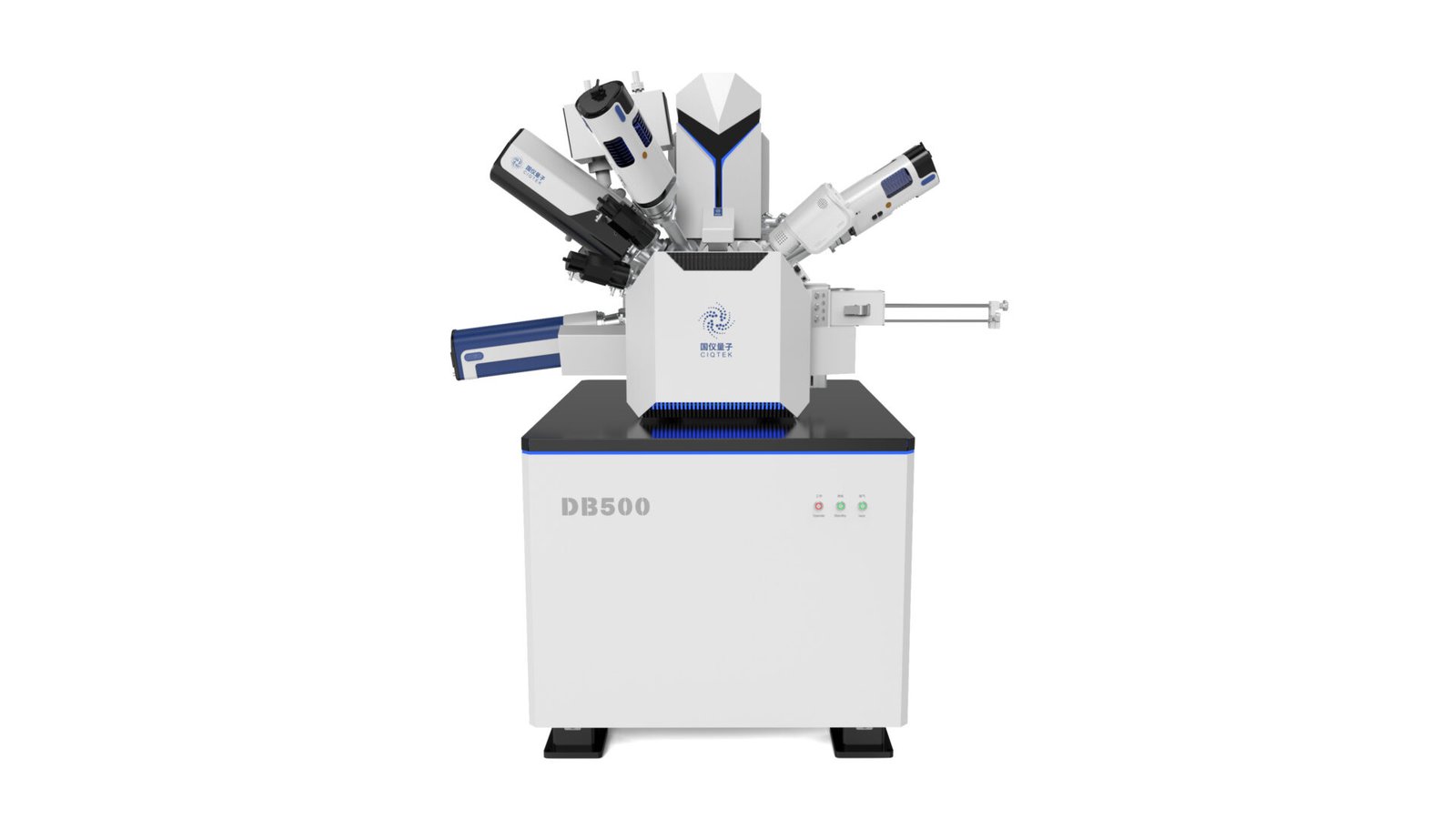
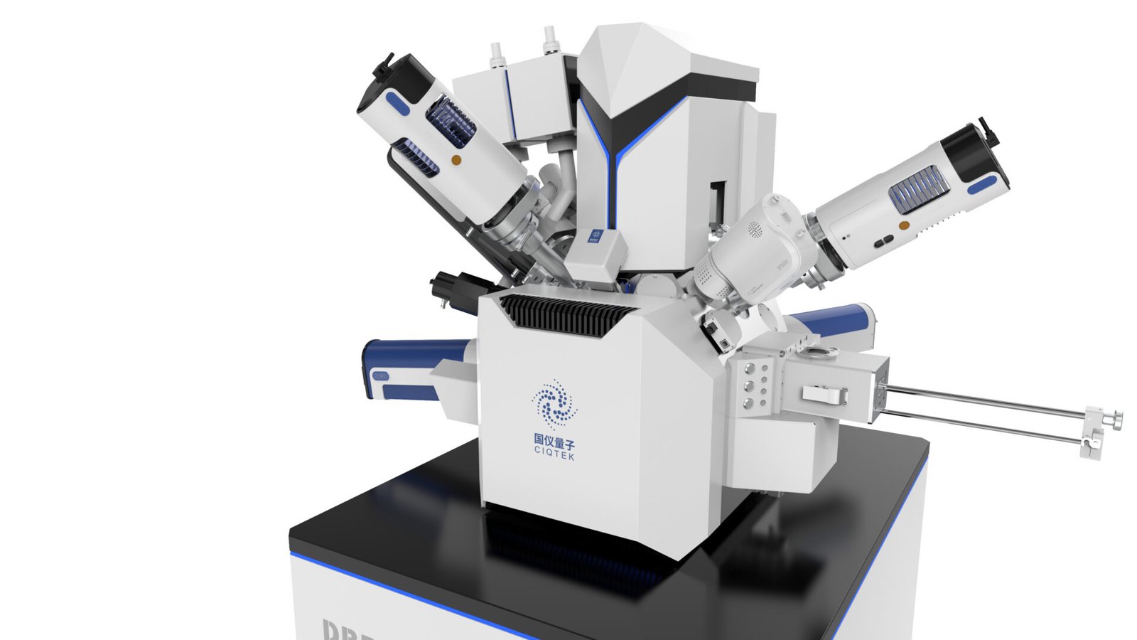
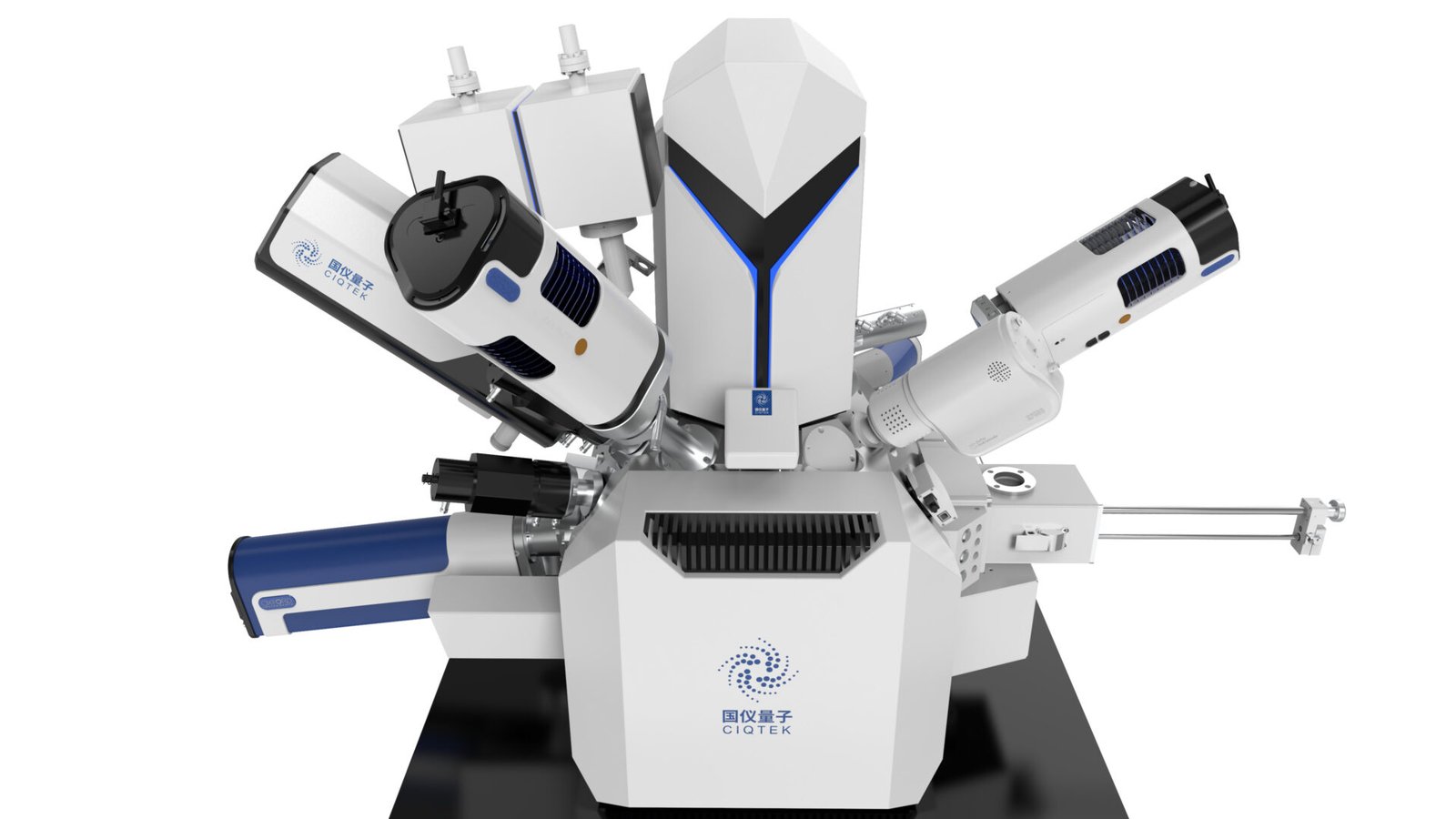
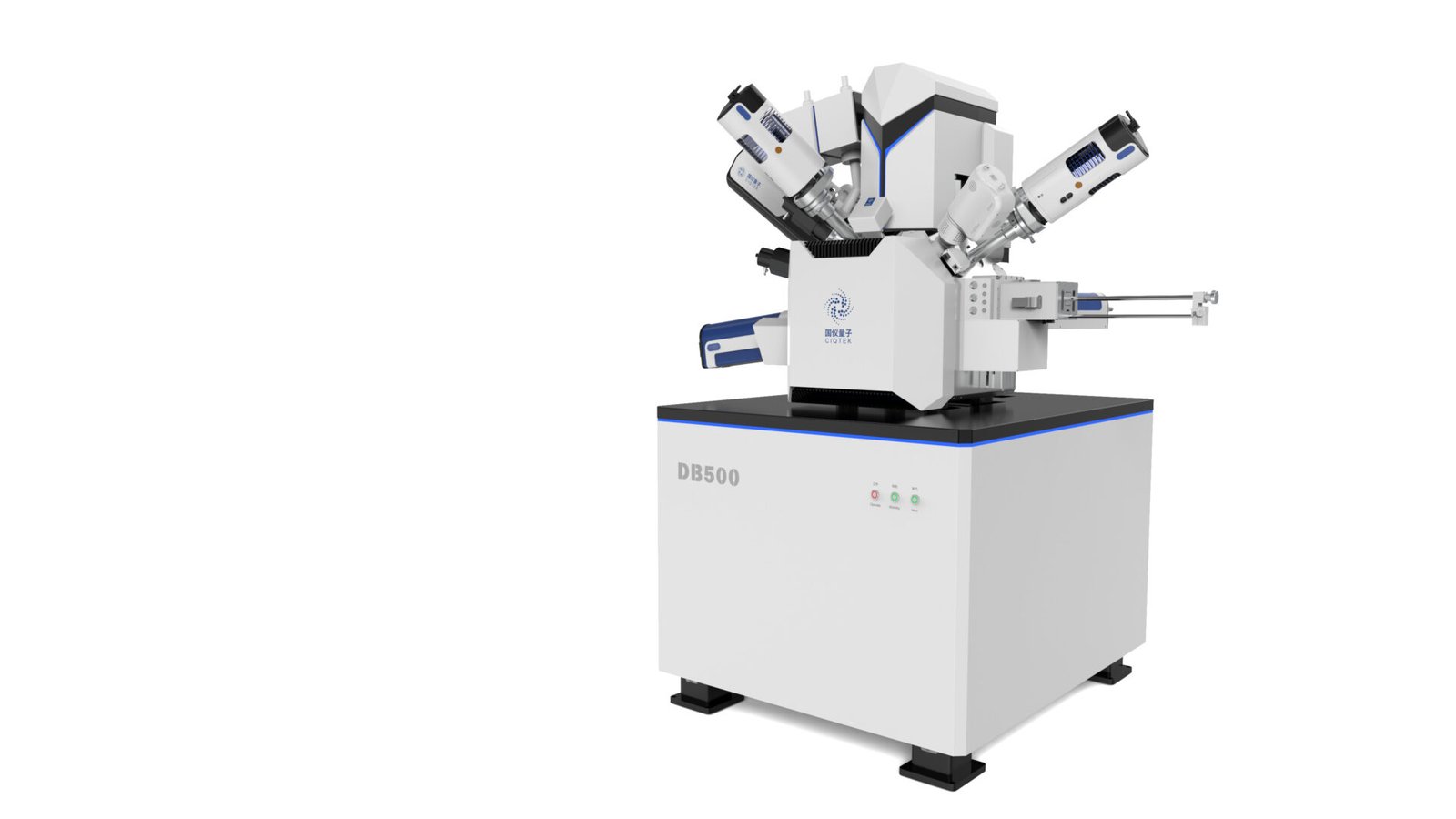
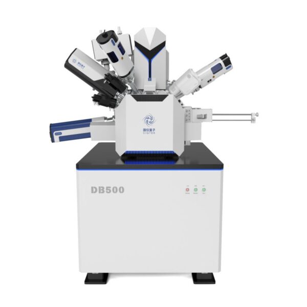
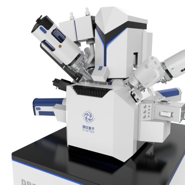
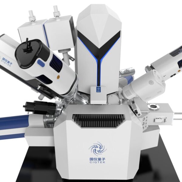
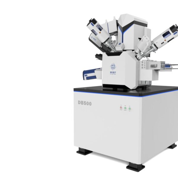
FIB-SEM has many applications, such as:
- Analyzing, depositing, and removing materials in a specific location, especially for semiconductors and materials science.
- Making thin and high-quality samples for transmission electron microscopy (TEM) from different kinds of materials.
- Visualizing and characterizing structures below the surface and in 3D by alternating FIB cutting and SEM imaging.
- Creating and designing devices at the nanoscale by FIB carving and adding.
[pdf-embedder url=”https://www.rigaslabs.gr/wp-content/uploads/2023/11/DB500-FIB-SEM-1.pdf” title=”DB500-FIB-SEM (1)”]